Summary of the simplest circuit scheme design of self-made power bank
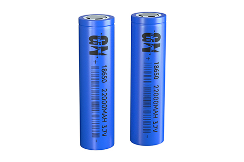
Lithium-ion batteries are currently the most widely used rechargeable
batteries. A single lithium battery can be used in low-power products, or
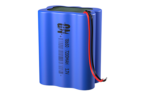
multiple lithium batteries can be connected in series and parallel to obtain
higher voltage and capacity. For example, a mobile power supply combines
multiple lithium batteries. Lithium batteries are connected in parallel to
obtain high capacity. Lithium batteries have the advantages of high energy
density, low self-discharge rate, no memory effect, long life, and light weight.
They are very suitable as a power source for portable products. The simplest
circuit design of homemade power bank (1)
As portable products continue to grow, the demand for mobile power supplies
continues to increase. Thin and compact, fast charging, high conversion
efficiency and high safety have also become the primary considerations for
consumers when purchasing mobile power supplies. In order to meet the needs of
consumers, many companies All have launched mobile power solutions. Here we use
the AIC6511 and AIC3420 developed by Peheng Semiconductor as design examples to
provide readers with reference.
A complete mobile power supply circuit includes battery charging management
IC, boost converter IC and MCU. Each part will affect the overall performance of
the mobile power supply, so it is very important to choose the appropriate IC.
Figure 4 shows the mobile power supply circuit to be introduced in this article,
which is mainly composed of AIC6511 lithium-ion battery charging converter,
AIC3420 boost converter and MCU. The proposed mobile power supply circuit will
be described in detail below.
Li-ion battery charging converter
Lithium-ion batteries are currently the most widely used rechargeable
batteries. A single lithium battery can be used in low-power products, or
multiple lithium batteries can be connected in series and parallel to obtain
higher voltage and capacity. For example, a mobile power supply combines
multiple lithium batteries. Lithium batteries are connected in parallel to
obtain high capacity. Lithium batteries have the advantages of high energy
density, low self-discharge rate, no memory effect, long life, and light weight.
They are very suitable as a power source for portable products.
Lithium battery charging ICs are divided into linear and switching types.
Linear charging ICs have low cost, fewer IC pins, and only require a few passive
components. However, linear charging ICs have large power losses. If the design
is not good, the IC temperature will often be too high. In addition, most mobile
power supplies use plastic casings with poor heat dissipation, making linear
charging ICs unable to provide large charging currents. Therefore, Linear
charging ICs are generally more suitable for low-capacity lithium-ion battery
applications. If you want to fully charge the battery in a short time, you must
increase the charging current. At this time, you can consider applying a
switching charging IC. Switching charging IC uses high-frequency switching of
switches to achieve energy transfer, can provide a large charging current, and
has high conversion efficiency without overheating. It is suitable for charging
applications of high-capacity batteries.
During the charging process, when the battery voltage rises to 4.2V, stop
charging immediately to avoid the danger of overcharging the battery. When the
battery is discharging, if the battery voltage drops below 2.5V, stop
discharging immediately to prevent the battery from overcharging. discharge and
reduce the battery life. In addition, the application of lithium batteries will
also include a short-circuit protection circuit to prevent the lithium battery
from causing danger due to short circuit.
Lithium batteries have very high charging requirements and require
sophisticated charging circuits to ensure the safety of charging. In particular,
the accuracy of the termination voltage is required to be within ±0.5% of the
rated value. Currently, the three-stage charging method is most commonly used
for lithium battery charging, namely pre-charging mode (TrickleChargeMode),
constant current charging mode (ConstantCurrentChargeMode), and constant voltage
charging mode (ConstantVoltageChargeMode). The charging IC will detect the
status of the battery before charging. If the battery voltage is greater than
3V, it will be charged in constant current charging mode; if the battery voltage
is lower than 3V, it will be charged in precharge mode (about 10% of the
constant current charging mode charging current) Charging, when it is close to
the end voltage, changes to constant voltage mode charging. At this time, the
battery voltage is almost unchanged, but the charging current will continue to
decrease. When the charging current drops to a certain value (about 10% of the
charging current in constant current charging mode ), the charging current will
be turned off and charging is completed. Figure 5 shows the lithium battery
charging characteristic curve using the three-stage charging method.
The simplest circuit design of homemade power bank (2)
I have an old laptop battery that I plan to recycle into a mobile power
bank. After disassembling the laptop battery, I measured it with a multimeter
and found that the voltage of two of the cells was 0V. It was estimated that the
laptop battery would not last long. This is the reason, so I removed the two
cells with a voltage of 0V. Throw it away. The schematic diagram produced is
shown below. Through the USB socket on the left side of the schematic diagram,
input 5V DC to charge the battery pack. After it is fully charged, you can carry
it with you and output 5V DC through the boost module that boosts 3.7V to 5V to
charge mobile phones and other devices.
Materials: 1 DC-DC boost module that boosts 3.7V to 5V, 1 switch, 1 USB
socket female socket, and some wires.
The production process is also relatively simple. Weld the connections
according to the schematic diagram, then use hot melt glue to fix the battery
pack, boost module, switch, and USB socket, and then fix them in the original
laptop battery box and you're done.
The simplest circuit design of homemade power bank (3)
Schematic diagram
The circuit board you buy online will have two wires written on it: +
(positive pole) - (negative pole). As shown in the picture;
Battery selection: It is best to use a lithium battery with a voltage of
3.7V. The voltage between the battery and the battery must be equal.
Just connect their positive and negative poles in parallel, remember to
connect them in parallel.
The simplest circuit design of homemade power bank (4)
Analysis of a mobile phone charger power conversion circuit
When analyzing a power supply, we often start with the input. 220V AC
input, one end passes through a 4007 half-wave rectifier, the other end passes
through a 10 ohm resistor, and is filtered by a 10uF capacitor. This 10 ohm
resistor is used for protection. If a fault occurs later and causes overcurrent,
then this resistor will be burned to avoid causing a larger fault. The 4007,
4700pF capacitor, and 82K resistor on the right form a high-voltage absorption
circuit. When the switch tube 13003 is turned off, it is responsible for
absorbing the induced voltage on the coil, thereby preventing high voltage from
being added to the switch tube 13003 and causing breakdown. 13003 is a switching
tube (the complete name should be MJE13003), with a voltage resistance of 400V,
a maximum collector current of 1.5A, and a maximum collector power consumption
of 14W. It is used to control the on and off between the primary winding and the
power supply. When the primary winding is continuously switched on and off, a
changing magnetic field will be formed in the switching transformer, thereby
generating an induced voltage in the secondary winding. Since the end of the
winding with the same name is not marked in the figure, it cannot be seen
whether it is a forward or flyback type.
However, from the structure of this circuit, it can be inferred that this
power supply should be a flyback type. The 510K at the left end is the starting
resistor, which provides the base current for starting the switch tube. The 10
resistor below 13003 is a current sampling resistor. The current is sampled and
turned into a voltage (its value is 10*I). This voltage is added to the base of
transistor C945 after passing through diode 4148. When the sampling voltage is
approximately greater than 1.4V, that is, when the switch tube current is
greater than 0.14A, transistor C945 is turned on, thereby pulling down the base
voltage of switch tube 13003 (clamping), thereby reducing the collector current,
thus limiting the switching current to prevent burning due to excessive current
(in fact, this is a constant current structure, which limits the maximum current
of the switch tube to about 140mA).
The induced voltage of the winding (sampling winding) on the lower left
side of the transformer is rectified by the rectifier diode 4148 and filtered by
the 22uF capacitor to form the sampling voltage. For the convenience of
analysis, we take the emitter end of the triode C945 as ground. Then the
sampling voltage is negative (about -4V), and the higher the output voltage, the
more negative the sampling voltage is. After the sampling voltage passes through
the 6.2V Zener diode, it is added to the base of the switch tube 13003. As
mentioned earlier, when the output voltage is higher, the sampling voltage
becomes more negative. When the negative reaches a certain level, the 6.2V Zener
diode is broken down, thereby pulling the base potential of switch 13003 low,
which will cause the switch tube to Disconnecting or delaying the conduction of
the switch controls the input of energy into the transformer, which also
controls the increase in the output voltage and realizes the function of
voltage-stabilizing output.
The 1K resistor and the 2700pF capacitor in series below are the positive
feedback branches. The induced voltage is taken out from the sampling winding
and added to the base of the switching tube to maintain oscillation. There is
not much to say about the secondary winding on the right. It is rectified by the
diode RF93 and filtered by the 220uF capacitor to output a voltage of 6V. I
couldn't find any information about the diode RF93. I guess it is a fast
recovery diode, such as a Schottky diode. Because the switching power supply has
a high operating frequency, a diode with an operating frequency is needed.
Common Schottky diodes such as 1N5816 and 1N5817 can be used here instead.
The simplest circuit design of homemade power bank (5)
When USB_IN has power access, pA6 changes from low to high, and an external
interrupt is used to wake up the MCU to enter charging work.
Input/output voltage detection
The charging mode can detect the external voltage through this detection
circuit. When the external voltage is higher than 5.5V, the pWM output is
forcibly turned off by the hardware and an interrupt is generated for
processing. In addition, since the input voltage source may be the USB port on a
general computer or the 5V output port of a wall transformer, the maximum
current supply capabilities of the two sources are different. This can be
determined by detecting the decrease in input voltage during charging. Input the
limit of the current supply capability of the source, thereby fixing the
charging current and no longer increasing it.
Read recommendations:
Alkaline D Battery LR20
Describe the main application fields of Lithium iron phosphate battery.CR1632 battery
Principle and application method of polymer lithium battery
801520 180mAh 3.7V
402030 lipo battery














 360° FACTORY VR TOUR
 Whatsapp
 Tel
Tel Email
Email TOP
TOP