Difference and selection analysis of transistors and MOS tubes in switching
power supply circuit design
How to distinguish and select transistors and MOS tubes in the design of
switching power supply circuits:
The working principle of the triode: The triode is a current amplifier
device with three poles, called the collector C, the base B, and the emitter E.
Divided into two types: NPN and PNP. We only take the common-emitter amplifier
circuit of an NPN triode as an example to illustrate the basic principles of the
triode amplifier circuit.
We call the current flowing from the base B to the emitter E the base
current Ib; the current flowing from the collector C to the emitter E is called
the collector current Ic. The directions of these two currents flow out of the
emitter, so an arrow is used on the emitter E to indicate the direction of the
current. The amplification effect of the transistor is: the collector current is
controlled by the base current (assuming that the power supply can provide a
large enough current to the collector), and a small change in the base current
will cause a large change in the collector current, and The change satisfies a
certain proportional relationship: the change in the collector current is β
times the change in the base current, that is, the current change is amplified
by β times, so we call β the amplification factor of the transistor (β is
generally much greater than 1, such as several Ten, hundreds). If we add a
changing small signal between the base and the emitter, this will cause a change
in the base current Ib. After the change in Ib is amplified, it will lead to a
large change in Ic. Transistors are current-controlled devices.
Mos transistor is a metal-oxide-semiconductor field effect transistor. Or
called metal-insulator-semiconductor. The source and drain of the MOS tube can
be swapped. They are both N-type regions formed in the P-type backgate. In most
cases, these two areas are the same, and even if the two ends are swapped, it
will not affect the performance of the device. Such devices are considered
symmetrical.
What happens when the gate (Gate) of the MOS capacitor is forward biased
relative to the substrate (BACKGATE). The electric field across the
GATEDIELECTRIC is strengthened, and more electrons are pulled up from the
substrate. At the same time, holes are repelled from the surface. As the GATE
voltage increases, there will be more electrons than holes on the surface.
Because of the excess electrons, the silicon surface looks like N-type silicon.
The reversal of doping polarity is called inversion, and the reversed silicon
layer is called a channel. As the GATE voltage continues to increase, more and
more electrons accumulate on the surface, and the channel becomes strongly
inverted. The voltage at which the channel is formed is called the threshold
voltage Vt. When the voltage difference between GATE and BACKGATE is less than
the threshold voltage, a channel will not be formed. So MOS is a voltage
controlled device.
(1) Field effect transistors are voltage control components, while
transistors are current control components. When only a small amount of current
is allowed to be taken from the signal source, a field effect transistor should
be used; when the signal voltage is low and a large amount of current is allowed
to be taken from the signal source, a transistor should be used.
(2) Field effect transistors use majority carriers to conduct electricity,
so they are called unipolar devices, while transistors have both majority
carriers and minority carriers to conduct electricity. It is called a bipolar
device.
(3) The source and drain of some field effect transistors can be used
interchangeably, and the gate voltage can be positive or negative, which is more
flexible than transistors.
(4) Field effect transistors can work under very low current and very low
voltage conditions, and its manufacturing process can easily integrate many
field effect transistors on a silicon wafer. Therefore, field effect transistors
are widely used in large-scale integrated circuits. has been widely used.
(5) Field effect transistors have the advantages of high input impedance
and low noise, so they are also widely used in switching power supplies and
various electronic equipment. In particular, using field effect tubes as power
drivers for switching power supplies can achieve performance that is difficult
to achieve with ordinary transistors.
(6) Field effect transistors are divided into two categories: junction type
and insulated gate type, and their control principles are the same.
There are many differences between transistor BJT and field effect
transistor FET. Here are a few:
1. The transistor is controlled by current, the MOS tube is voltage
controlled, the BJT amplifies the current, and the FET converts the gate voltage
into a drain current. The first parameter of BJT is the current amplification
factor β value, and the first parameter of FET is transconductance gm;
2. Driving capability: MOS tubes are often used in power switching tubes
and high-current local switching circuits;
3. Cost issue: triodes are cheap, MOS tubes are expensive;
4.BJT has poor linearity and FET has better linearity;
5.BJT has larger noise and FET has smaller noise;
6. There are only two types of BJT polarity: NPN and PNP. FET polarity
includes N-channel, P-channel, depletion mode and enhancement mode, so FET
selection and use are more complicated;
7. Power consumption problem: BJT has a small input resistance and consumes
a large current; FET has a large input resistance and consumes almost no
current;
In fact, transistors are relatively cheap and easy to use, and are often
used in digital circuit switching control; MOS tubes are used in high-frequency
and high-speed circuits, large current situations, and places that are sensitive
to base or drain control current.
Generally speaking, it is a major trend for FET to replace BJT in both
discrete component circuits and integrated circuits.
Read recommendations:
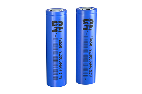
18650 2600mAh 3.7V
New energy trams are cost -effective to surpass oil vehicles?lifepo4 battery for solar energy storag
Graphene battery technology principle.lithium battery energy storage Processing
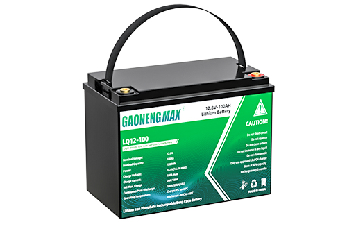
12v lithium ion battery pack 100ah
AG7 battery





























 360° FACTORY VR TOUR
 Whatsapp
 Tel
Tel Email
Email TOP
TOP