Solar cells are the core device in the pV power generation system. They use
the principle of photoelectric conversion to convert the sun's radiant light
into electrical energy through semiconductor materials. This photoelectric
conversion process is usually called the "photovoltaic effect", so the sun
Batteries are also called "photovoltaic cells". The semiconductor material used
in solar cells is a special substance between a conductor and an insulator.
In order to reduce the manufacturing cost of solar cells, scientists follow
two paths: one is to develop novel solar cell materials, and the other is to
improve the conversion efficiency of the solar cells themselves. The core
technology to convert inexhaustible sunlight into electrical energy for the
benefit of mankind is the photoelectric conversion rate of solar cells.
There are more than a dozen known semiconductor materials used to make
solar cells, so there are many types of solar cells. At present, the solar cell
with the most mature technology, commercial value and the widest market
application is silicon solar cell.
How to make solar cells
1. Silicon wafer cutting and material preparation:
The monocrystalline silicon material used in the industrial production of
silicon cells generally uses solar-grade monocrystalline silicon rods made by
the crucible Czochralski method. The original shape is cylindrical, and then cut
into square silicon wafers (or polycrystalline square silicon wafers). The side
length is generally 10~15cm, and the thickness is about 200~350um.
P-type with a resistivity of about 1Ω.cm (boron-doped).
2. Remove the damaged layer: Silicon wafers will produce a large number of
surface defects during the cutting process, which will cause two problems.
First, the surface quality is poor. In addition, these surface defects will lead
to an increase in debris during the battery manufacturing process. Therefore, to
remove the cutting damage layer, alkali or acid etching is generally used, and
the thickness of the etching is about 10um.
3. Velvet making:
Texturing is to etch the surface of the relatively smooth raw material
silicon wafer through acid or alkali etching to make it uneven and rough,
forming diffuse reflection and reducing the loss of solar energy directly
hitting the surface of the silicon wafer. For single crystal silicon, the method
of NaOH and alcohol is generally used to etch. The anisotropic corrosion of
single crystal silicon is used to form numerous pyramid structures on the
surface. The temperature of the alkali solution is about 80 degrees, the
concentration is about 1~2%, and the etching time is About 15 minutes. For
polycrystalline, acid etching is generally used.
4. Diffusion junction making: The purpose of diffusion is to form pN
junction. Phosphorus is commonly used for n-type doping. Since solid-state
diffusion requires high temperatures, it is very important to clean the surface
of the silicon wafer before diffusion. The silicon wafer is required to be
cleaned after texturing, that is, acid is used to neutralize alkali residues and
metal impurities on the surface of the silicon wafer.
5. Edge etching and cleaning:
During the diffusion process, a diffusion layer is also formed on the
peripheral surface of the silicon wafer. The peripheral diffusion layer forms a
short circuit ring between the upper and lower electrodes of the battery and
must be removed. Any small local short circuit on the periphery will reduce the
parallel resistance of the battery and even become a waste product. At present,
industrial production uses plasma dry etching, which uses fluorine and oxygen to
alternately act on silicon under glow discharge conditions to remove the
periphery containing the diffusion layer. The purpose of post-diffusion cleaning
is to remove the phosphosilicate glass formed during the diffusion process.
6. Deposit an anti-reflective layer: The purpose of depositing an
anti-reflective layer is to reduce surface reflection and increase the
refractive index. pECVD is widely used to deposit SiN. When pECVD deposits SiN,
it not only grows SiN as an anti-reflective film, but also generates a large
amount of atomic hydrogen. These hydrogen atoms can have dual effects of surface
passivation and body passivation on polycrystalline silicon wafers. It can be
used for mass production.
7. Screen printing upper and lower electrodes: The preparation of
electrodes is a crucial step in the solar cell preparation process. It not only
determines the structure of the emitting area, but also determines the series
resistance of the battery and the area of the battery surface covered by metal.
Vacuum evaporation or chemical plating technology was first used, but now the
screen printing method is commonly used, that is, silver paste aluminum paste
(silver aluminum paste) is printed on the front and back of the solar cell
through a special printer and template to form the positive and negative
electrodes lead.
8. Co-firing to form metal contact: Crystalline silicon solar cells need to
print metal paste three times. The traditional process requires two sinterings
to form a good ohmic contact with metal electrodes. The co-firing process only
requires one sintering to form the upper and lower electrodes at the same time.
of ohmic contact. In the production of screen-printed electrodes for solar
cells, chain sintering furnaces are usually used for rapid sintering.
9. Battery chip testing: The completed battery cells are classified into
different categories after testing.
Read recommendations:
Ni-MH AA1000mAh 1.2V
Lithium battery core technology
3.2v 30ah lifepo4 battery cell.Power lithium batteries gradually reach production capacity, and lith
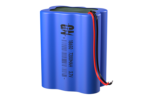
701224 lipo battery company
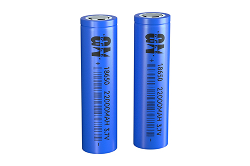
18650 battery pack 12v

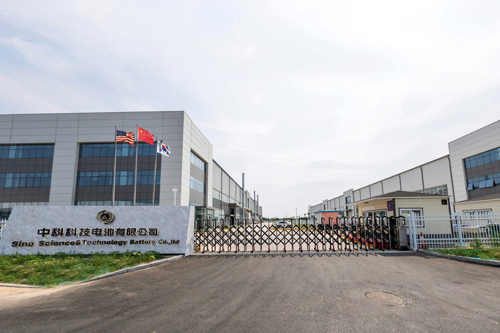
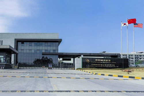


 360° FACTORY VR TOUR
 Whatsapp
 Tel
Tel Email
Email TOP
TOP