Research on button battery cr2032 management chip and its low power design - low power consumption of mixed analog and digital circuits
2.1 Low power design of digital circuits
2.1.1 Power consumption model and influencing factors of digital circuits
Taking the most basic inverter unit shown in Figure 2.1.1 as an example, the power consumption of CMOS digital circuits can be divided into two parts: static power consumption and dynamic power consumption:
Among them, static power consumption
In the formula, the first term is the static power consumption caused by the DC short-circuit current ISC when p1 and N1 are turned on at the same time; the second term is caused by leakage current, including subthreshold current and leakage current when the source and drain regions are reverse biased with the substrate.
Dynamic power consumption is consumed by charging and discharging the equivalent load capacitance of the circuit node, also known as switching power consumption, which can be expressed as
In the formula, α0→1 is the switching activity factor, which indicates the number of state transitions in each clock cycle. Its size is related to the circuit structure, logical function, input signal state and the initial state of the node. Generally, α0→1≤1 in CMOS circuits; CL is the equivalent load capacitance; ƒ is the clock frequency; VDD is the power supply voltage.
In the power consumption of CMOS circuits of 0.18μm and above, dynamic power consumption is dominant, and sometimes short-circuit power consumption must be considered. In general, leakage current and steady-state bias current power consumption can be ignored. Therefore, to reduce circuit power consumption, it is necessary to start with reducing dynamic power consumption. It can be said that formula (2.1.3) is the guiding formula for low-power digital circuits.
Formula (2.1.3) shows that there are four ways to reduce the dynamic power consumption of the circuit:
First, reduce the switching activity factor α0→1. In each clock cycle, not all nodes change state, and not all state transitions consume energy (such as the state transition from 1 to 0). Therefore, the essence of reducing the switching activity factor is to reduce unnecessary energy-consuming transitions by optimizing algorithms, logical structures, etc. according to the combination of input signals. Commonly used methods include gated clock technology, power estimation/optimization CAD technology, and transition reduction coding technology. Since it is very difficult to estimate α0→1 quickly and accurately, it is urgent to develop practical power consumption estimation CAD technology; secondly, reducing α0→1 to reduce dynamic power consumption is very effective and has great potential, so this is also one of the important aspects of low power consumption research.
Second, reduce the equivalent load capacitance CL. CL is mainly composed of two aspects: on the one hand, the input gate capacitance of the subsequent gate and the capacitance of the source and drain region of the inverter, which are related to the device process; on the other hand, the interconnection line capacitance.
Therefore, to reduce CL, you can use methods such as optimizing logic circuits (such as reducing the number of transistors used), optimizing transistor size, reducing the capacitance of high activity factors in process mapping, and reasonable layout in the layout. It can be said that at all levels of design, the impact of CL on power consumption must be considered.
Third, reduce the operating frequency f. If the power consumption is reduced only by reducing the frequency of the circuit, it must be at the expense of speed. Therefore, the strategy of clock (frequency) management is to use multi-frequency technology, that is, to allocate different frequencies in different system parts, or optimize the clock tree (ClockTree) when designing the layout, while ensuring that the main frequency of the circuit remains unchanged, to reduce dynamic power consumption as much as possible.
Fourth, reduce the working power supply voltage VDD. Since power consumption is proportional to the square of the power supply voltage, this is also the most effective way to reduce power consumption. However, under the condition of process size determination and first-order approximation, the circuit delay and VDD satisfy the following formula
That is, Td∝(CdVDD)/(VDD-VTH)2, where W and L are the gate width and gate length of the device, μ is the carrier mobility, COX is the oxide layer capacitance, and VTH is the MOS tube threshold voltage.
As shown in Figure 2.1.2, from the relationship between circuit energy, delay and working voltage, it can be seen that when VDD is in the range of 2.5VTH to 6VTH, the delay and energy delay product change relatively slowly, and when VDD=3VTH, the two reach the lowest value. When the working voltage continues to drop to close to VTH, the delay will rise sharply.
In order to improve the circuit speed reduction caused by the decrease of VDD, a parallel or pipeline structure can be used, but this will increase the circuit area; another compensation method is to increase the VDD/VTH value by reducing VTH, but at the same time the circuit leakage current will increase, which can be solved by variable voltage and variable threshold voltage technology; in some non-critical circuits, multi-voltage and multi-threshold voltage technology can also be used to compensate.
2.1.2 Low-power design method of digital circuit
In the current ASIC design process, the top-down process is often used. The optimization of power consumption can also be considered. At different design levels, the above factors affecting power consumption are selected purposefully to achieve the goal of minimizing power consumption under given performance constraints.
From the abstract level, low-power design can be divided into: system level, structure level/algorithm level, register transfer level, logic/gate level and layout level. At different levels of design, the factors affecting power consumption have different uses, so the effect of power consumption optimization is also different; comprehensively speaking, the earlier low power consumption is considered in chip design, the more significant the effect will be.
1 System and structure level
At this level, starting from the system function, it is divided into two types: static low-power design and dynamic power management (DpM) technology. Static low-power design is to use different circuit structures and different encoding methods to achieve low power consumption in the design stage (such as synthesis and editing) when considering the specific implementation of the system; while dynamic power management technology is closely related to the behavior during operation. It must fully consider the relationship between the system and the task or the load, make corresponding decisions, and achieve low power consumption.
1) Static low-power method
① Circuit structure
The parallel structure is to divide a data processing function module into several identical sub-modules, process data in parallel, and then select the corresponding output. This method allows the voltage, frequency and other factors of each sub-module to be reduced while keeping the total module speed unchanged, so as to reduce the total power consumption, but at the cost of adding new chip area.
The pipeline structure is to segment the data and continue to process it slowly while keeping the overall speed unchanged, and the speed margin can reduce power consumption by reducing the voltage. If combined with the parallel structure, better power saving effect can be achieved.
② Voltage technology
Similar to improving circuit structure, voltage technology is also used to compensate for the speed drop caused by the reduction of working voltage [26, 27]. Multi-voltage technology is aimed at different performance requirements. Different parts of the system also use different working voltages to save power, but this requires an additional on-chip voltage converter.
③ Coding optimization
In the commonly used binary coding, all idle high bits are used as sign extension bits, which will add energy-consuming jumps. The sign-value coding method (such as Gray code, etc.) only uses the highest bit to represent the symbol. If it is used instead of binary coding, the power consumption caused by data symbol changes can be reduced.
2) Dynamic power management technology
It is an effective means of system-level power optimization. According to the load request, the subsystem can be divided into working and idle modes. In idle mode, the subsystem can be turned off and enter the low-power standby (Standby)
and the energy-free sleep (Sleep) state; otherwise, the subsystem is awakened and enters the normal working mode.
This selective shutdown of idle subsystems has a significant effect in reducing power consumption. For example, in PC system-level power management, the most common method is to shut down hard disks and displays that are not executing tasks to save power.
The limitation of this method is that there is usually a delay in the process of switching power states, and waking up subsystems in sleep state also requires more energy. Therefore, DPM technology needs to solve the following problems: first, when to shut down the subsystem and how long to shut it down; second, whether it is worth shutting down, that is, whether it takes more energy to restore the state. These are the contents to be studied in the decision strategy. The most commonly used methods can be divided into three types: timeout-based method, predictive-based method, and stochastic-based method.
Different from the above-mentioned change in the power state of the subsystem, the dynamic voltage scaling (DVS) technology predicts the system load based on the system's working state based on intervals (Interval-based) or threads (Thread-based) [33, 34], and dynamically changes the system's working voltage. Dynamic Voltage and Frequency Scaling technology changes the working voltage and frequency at the same time to obtain the lowest system power consumption.
Compared with static low-power design, DpM technology needs to predict the relationship between the system and the load, the system and the power supply, and dynamically adjust the working state, voltage and frequency. The modeling and prediction algorithm of the system working state are more complicated, and more work is urgently needed, but it is certain that the effect of DpM technology in reducing power consumption is more significant.
2 Register transfer level
As a high-level structure of synthesis (sorting and allocation), the RTL level will include a control part (also called a controller) and an operation part (also called a data path), as shown in Figure 2.1.3.
The data path is characterized by registers, and the controller is implemented by combinational logic. Therefore, the object of RTL-level low-power design will be timing and combinational logic, which can be implemented using hardware description languages VHDL and VERILOG. In addition, the abstract level of RTL determines that it cannot involve power supply voltage and capacitance. Therefore, the important way to reduce power consumption is to reduce the switching activity factor, that is, to reduce the jump frequency of registers and combinational logic.
1) Operands
At the RTL level, operand isolation is the most commonly used low-power technology for combinational logic. Its essence is to add a latch between combinational logic modules. When the latch is enabled, the register value is not updated and the combinational path is isolated [36, 37]. Only when valid operations are performed will the combinational logic have energy-consuming jumps, which reduces the power consumption of this module.
Operand transformation is sometimes also called data path reordering, which refers to the technology of reordering circuit units to reduce power consumption without affecting the logical function, with the strategy of minimum flip frequency.
2) Gated clock technology
Currently, gated clock technology is considered to be one of the most effective methods to reduce power consumption. The objects controlled can not only be registers, latches, clock generation circuits, etc., but also subsystems can be controlled by gated clock distribution.
Taking registers as an example, the basic idea of gated clock is to control the clock through a gated or enable signal, that is, a "gated clock" signal appears at the output of the so-called gated clock unit, replacing the original clock input signal of the register. When the register is temporarily not working, the gated clock puts the register in a non-triggered state, thereby blocking the update of the input data and reducing invalid switching activities. In the gated clock unit shown in Figure 2.1.4, latches are often used to prevent glitches when the enable signal propagates to the output.
It should be pointed out that when the clock frequency increases, the influence of clock skew (ClockSkew) will not be ignored, which will increase the complexity of the clock tree design; considering the additional power consumption of the control circuit of the gated clock logic, the gated clock technology is suitable for application at a higher level of abstraction; in addition, when the leakage current power consumption is dominant, the gated clock is not very useful.
3 Logic/gate level
The important feature of these two levels is that advanced low-power technologies can be applied in a wide range. In the process of logic optimization, some technical parameters such as power supply voltage are fixed. When a given logic is to be implemented, the design freedom can be in selecting functions and determining the size of gate units. There are many literatures that study two levels of low-power technology.
1) Local transformation technology: Local transformation (localTransformation)
Including technology mapping (TechnologyMapping), pin permutation (pinpermutation), state assignment (phaseassignment) and other methods, usually applied to the gate netlist, and for nodes with large switching capacitance. The basic idea is: near the target node, replace one or several gate units to reduce capacitance and switching activity factors. However, this method must pay attention to the balance between short-circuit current and output power consumption.
In the logic synthesis stage, the commonly used transformation technology is process mapping, which aims to map a logic network optimized by a process-independent optimization program to a target library of pre-defined gate units. The mapping strategy is as follows: First, map nodes with high switching activity factors to internal nodes of the unit to reduce the capacitance value; second, the selection of gate unit size must be a compromise between the unit's driving capability and power consumption; third, in the process mapping method related to power consumption, small delays and area mapping must also be considered. In order to further reduce power consumption, before process mapping, the original circuit with complex nodes is usually decomposed into a series of gate units with basic functions, which is called process decomposition (Technology Decomposition); when a circuit is mapped, it can also optimize power consumption by reducing unnecessary large-sized gate units and logically equivalent pin arrangements through gate resizing and pin transformation.
State allocation is to add inverters between nodes to invert the input signal of the operation and also invert the output. This gate-level conversion technology reduces power consumption in the following ways: First, the added inverter adds other conversion opportunities and can make considerable changes with the original adjacent inverters, such as merging, canceling, etc.; second, this method can remove the inverter on the node path with high switching activity factor, thereby having lower power consumption.
2) The pre-computation method refers to the method of adding a pre-computation logic circuit to the original circuit. The basic idea is: selectively estimate the logic output value of the circuit in advance one clock cycle, and in the next cycle, turn off some units inside the circuit to reduce the switching activity factor and capacitance of the node to reduce power consumption.
3) New logic circuit structure The type of logic structure is closely related to the power consumption, area and speed of the circuit. In order to obtain lower power consumption, many literatures have studied the optimization of logic structure.
CpL (passTransistorLogic) is a low-power logic circuit that has been studied more. It uses two sets of NMOS transmission gates to realize mutualThe two pMOS transistors are used as feedback transistors to pull up the high level transmitted by the NMOS transmission gate to the power supply voltage. The advantages of the CpL circuit are small input load and strong output driving capability. The disadvantages are that there are many inherent nodes, many connections, and great wiring difficulty.
Dynamic logic circuits have lower power consumption, especially dynamic differential logic, which has received attention because of its higher noise suppression characteristics. Reference [49] proposed a study on limited swing logic (Swing Limited Logic, SLL), which can achieve high performance under a given power supply voltage, and the energy delay product is one order of magnitude lower than that of traditional circuits.
4 Layout level
1) Layout and routing In low-power layout design, reasonable layout and routing are the key. Traditional layout and routing focus on area and delay, so they often pursue the shortest wiring and the smallest capacitance; while the layout and routing method for low power consumption not only considers the traditional design goals, but also combines with the signal activity in the design, with the signal activity and the capacitance product minimized as the optimization goal to achieve low power consumption [50].
2) Clock tree design In layout design, the timing circuit is a key point to reduce power consumption. In synchronous systems, clocks usually consume a large part of the total energy; in different design goals, the power consumption of clock generation and clock distribution can account for 30% or even 40% of the system power consumption. At this stage, the clock network distribution, that is, the optimization of the clock tree structure, and the selection of the driving method, can achieve a compromise between node delay and power consumption by using buffer insertion optimization and variable line width optimization. In addition, given the important impact of clock deviation on circuit performance, under the premise of ensuring circuit timing, a specific non-zero deviation clock tree can be used to obtain beneficial power reduction and improvement of clock frequency and circuit stability.
Read recommendations:
702535 600mAh 3.7V
Demand market demand for iron phosphate lithium batteries in communication base stations
Application Areas of Lithium - Polymer Batteries
AA Ni-MH batteries manufacture
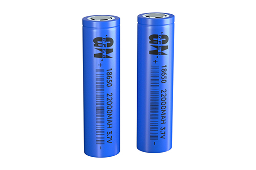
3.7v battery 18650


 360° FACTORY VR TOUR
 Whatsapp
 Tel
Tel Email
Email TOP
TOP